An HF Power Amplifier with Real RF Transistors
As I near construction of a full-suite transceiver, I’m prototyping each of the major components to make sure they’re likely to work. This post is about a simple class-C power amplifier; different from my other ones I’ve blogged about, this is a pretty straightforward design, but with one important twist. I’m actually using transistors that are designed for RF power amplifier applications. I know, I know… sounds crazy, but it came out really well!
Rationale
This first transceiver is going to be a CW thing, so I don’t need a fancy linear amplifier. I enjoyed playing with IRF510s, don’t get me wrong… but someone I respect told me I should just use actual RF transistors. I know it’s somewhat against the ham radio ethic to just pay for a part that does what you’ll use it for (I’ve heard that the IRF510 is found at the intersection of ham frugality and the desire to push a square peg through a round hole) :-).
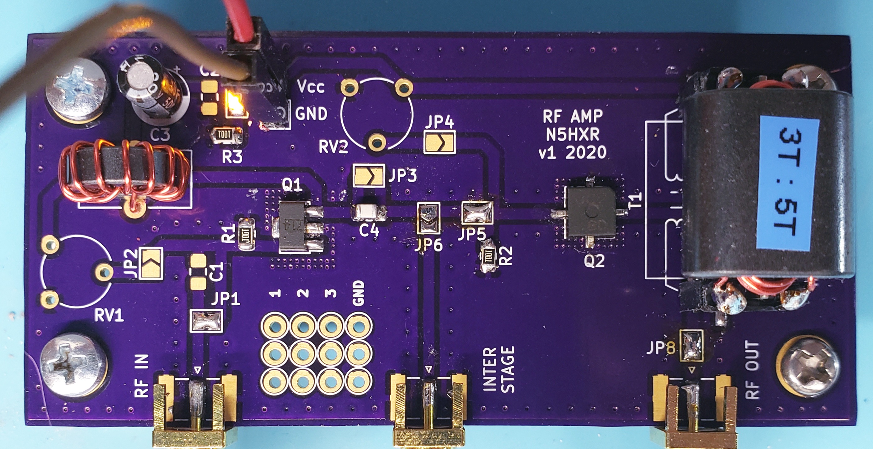
But I had to try it! This is the essential schematic, though I put it together on a sort of generic PA experimenting PCB I put together some time ago, but never got around to using:
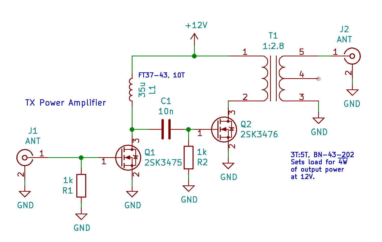
This is about as simple as it could possibly be – the 2SK3475 is intended for driver amplifier applications, and is supposed to be good for about 15dB of gain at UHF frequencies, per the datasheet. I asked some folks once if it would be bad to use such an animal for HF, and was warned there might be too much gain, or I might have oscillation issues, but no one I could find knew for sure. It seemed like just the thing worth trying! Anyway, the driver is designed to put out about 600mW of power.
I want a little more than that, so I paired it with the 2SK3476. It’s a much beefier package, intended for about 11dB of power gain at UHF, targeting the handheld transceiver market, rated to about 7W of output power. In the schematic, I load it with a somewhat conservative 18 ohms through the 3T:5T transformer. I figure that should get me about (24*0.3535)**2/18 watts, which comes out right about 4W, assuming I can drive it fully on and off.
Construction
I started by building out the driver stage, with the 2SK3475. It went smoothly, and I hooked it up with my QRP Labs Progrock for the RF input. The Progrock is an Si5351-based oscillator, so it puts out about 8-10mW. The result was a very nice 400mW of output, without doing anything extra for impedance matching or adjusting the load on the transistor. That means I was getting about 16dB of power gain – more than the 14dB in the datasheet, but nothing crazy. More importantly, I didn’t see any unwanted oscillations or concerning power draw that would indicate deeper issues. I was very happy with it.
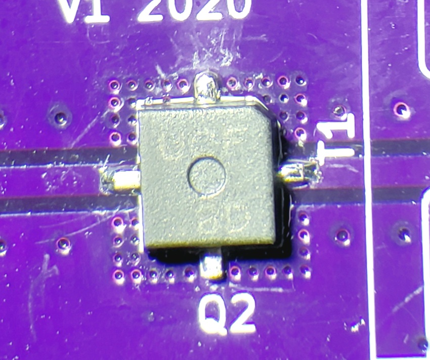
Continuing onward, it was very hard to solder on the 2SK3476 – the footprint I made up for it has lots of through holes for thermal management, and with the pad completely surrounded by the package, I simply couldn’t do it with an iron. I had to break out the hot air rework station, and solder it with air. I used a large soldering iron tip to cover the pad with solder, balanced the transistor on the solder blob, and heated it with the air until it pulled down tight to the board. It actually went really well, I thought!
The final result was as pictured at the beginning of this post. I ended up using this professionally produced PCB because I knew the ground plane, thermal vias, and other features I could get from a fab were going to be important for this to work well. I would guess that if I had cut a single layer board on the mill, I’d be much more likely to encounter difficulties!
Testing
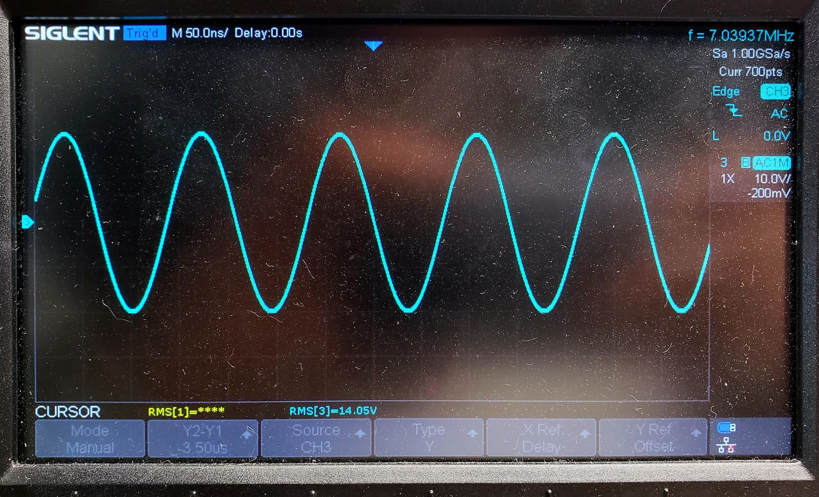
I rigged everything up with the Progrock as the RF generator, powered with 12V, and through a 7th order low pass filter for the 40m band. It’s pretty important in class C to have some resonant circuit in front of the final transistor to round out the waveform – that may as well be an LPF too, so it can eliminate the harmonics in the same stroke. The RF output from the amplifier board goes to my oscilloscope, and is terminated with a nice big dummy load:
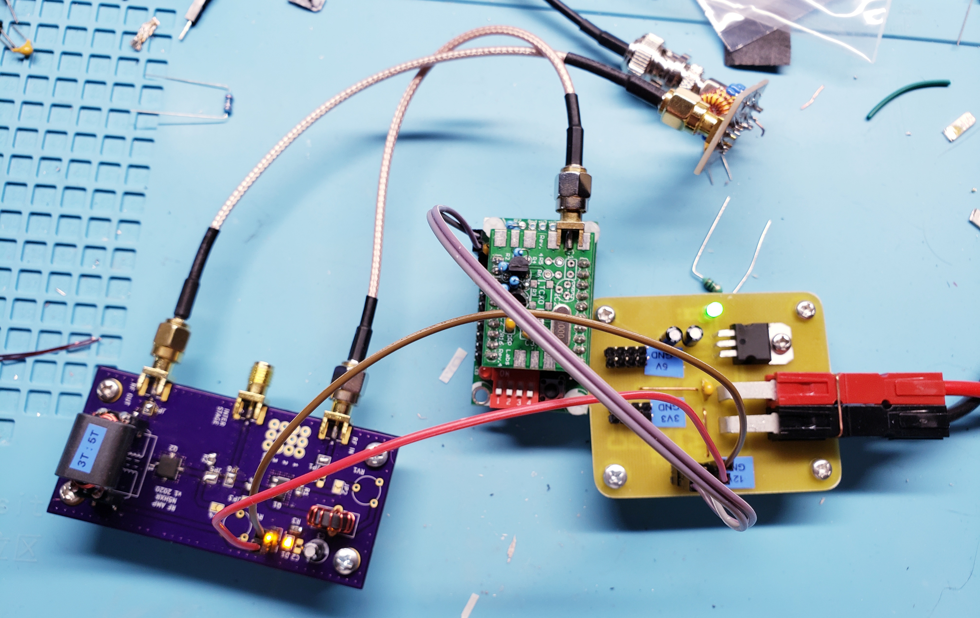
And after setting things up on the oscilloscope, I was greeted with this beautiful waveform. An excellent signal, at 3.95W. Even better, the amplifier board drew only 509mA, which comes out to 6.1W. So, 3.95/6.1 ends up being 65% efficient. Quite reasonable for class C and just a quick and simple arrangement. I suppose it should be up around 75%, but I might need to adjust some things in the circuit to eke out the most efficiency.
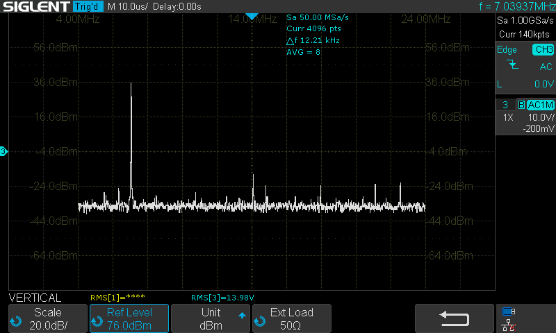
Checking with the FFT feature on the oscilloscope, I could see that the 7th order LPF was doing its job. All harmonics at better than -53dBc – legal for use on the air!
I was curious about how well things were going thermally, so I let it run for 5 minutes straight, and looked at it through the thermal camera:
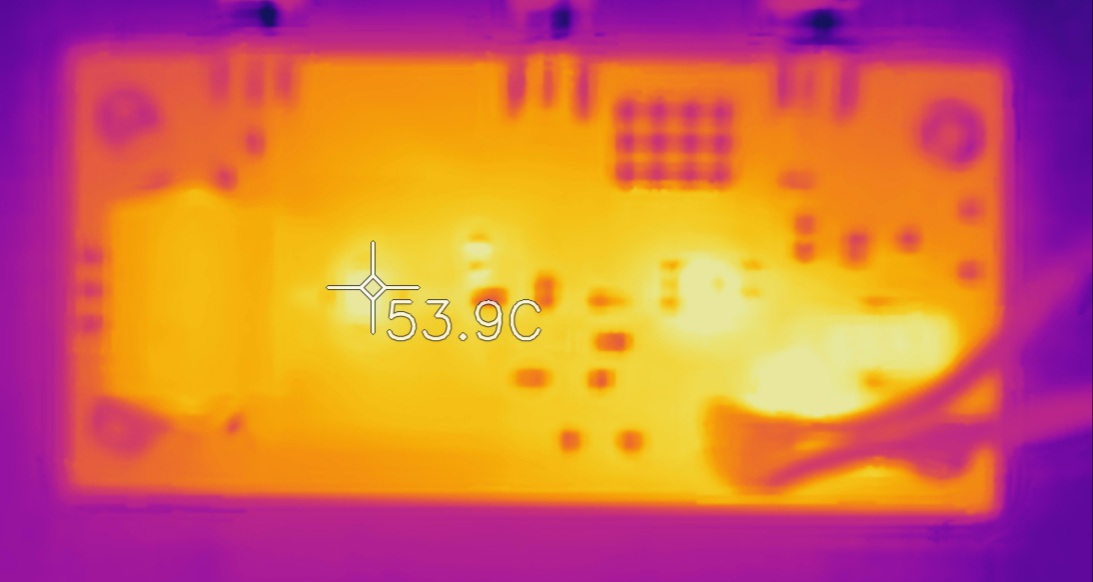
Really not bad at all! Getting into the 50s is certainly pretty warm, but not “death of the transistor” warm :-). And with 100% duty for five minutes, I figured this was a pretty good idea of “worst case”. I believe I could get away with using a PA along these lines without any extra heat-sinking, depending on the enclosure and ventilation.
Conclusion
OK, I have to admit… using parts for their intended purpose is pretty awesome. These RF transistors are designed for battery voltage levels, have low gate capacitance, and are intended for grounded source operation with a minimum of fuss.
Compared to all the fussing that goes on with IRF510s, I think this was pretty eye-opening for me. It calls to mind all the frustration I had trying to make small-signal transistors work as power amplifiers as well. Square pegs and round holes!
I think I’ll plan to use something like this for my upcoming transceiver board. Might not even try to tweak the efficiency up – 65% is pretty good for a newb’s first transceiver ;-).