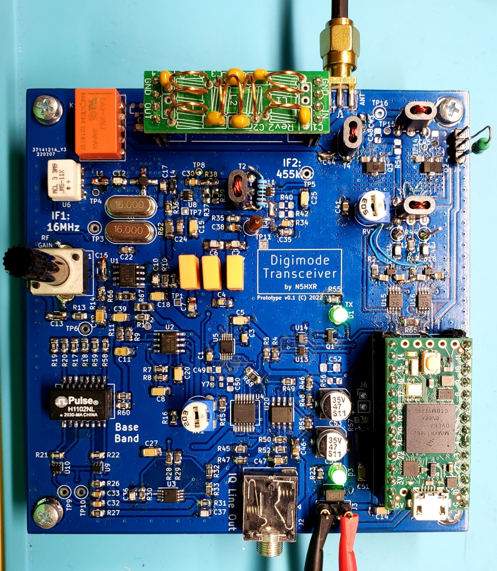
Digimode Playground Transceiver
I’ve harmonized some of my thinking around the various experiments I’ve done recently, and decided I was ready to bring a bunch of ideas together in a big experiment. This post details my adventure trying to use the full 10x10cm of a JLC PCB order… or… how I made a double conversion superhet SDR transceiver and learned a whole lot!
Level set expectations
So, right off the bat it’s important I make it very clear that I’m not an expert by any means! A lot of what went into this build is pure fantastical experimentation. In some cases I just wanted to see if an idea would work; and other ideas got scrapped during construction because they turned out not to (hah). So some of this is a sort of comedy of rookie mistakes… but it’s also a genuine step in my journey, and it does actually work fairly well after all!
Developing the concept
I’ve built some IQ modulators and demodulators, and played with some crystal filters. Instead of making yet another direct conversion transceiver, I thought perhaps it was time to build a superhet. And for extra complexity, I thought I’d make it two conversions, just to settle that I understand the concept.
I also wanted to order a fancy PCB from JLC for this one… and recognizing that the cost is the same up to 10x10cm, I realized that just a superhet receiver section would take up a very small portion of that space. I could maybe add on a little TX section to test following up my IQ modulator I’d built with an RF power amplifier… And then if I do that, I may as well throw a footprint to put a powerful microcontroller on and see if I can do onboard modulation and demodulation.
And so, one step after another, the concept grew into a full-suite transceiver idea. I ended up with the following major features in view:
- Dual conversion superhet design
- Teensy 4.0 microcontroller for the brains
- IQ audio baseband for ADC processing
- Manual adjustable RF gain
- DAC-driven IQ modulator for TX
- Push-pull RF power amplifier built on 2SK3475
- Pluggable QRP Labs LPF modules to make it multiband
- TRS output for AF output to a computer or external device
For the IFs, I chose a first IF of 16MHz, which I felt would give me some good range for high-side conversion and knock down image signals very effectively, using a crystal roofing filter. Being solidly HF at that point, then I figured I’d use a MMIC for IF gain, and experiment with a few new parts.
But, since it’s not so easy to make a really narrow 16MHz filter for in-band filtering, I then convert that down to 455kHz to use a ceramic filter for selectivity. Being a fairly low frequency, I realized I could use a mid-range opamp for gain at this stage, and this presents the opportunity to easily build in variable RF gain.
Finally, for the conversion to AF baseband, I use a switching IQ mixer into some AF gain stages intended to set levels appropriately for processing in a 3.3v microcontroller.
It seemed reasonable to target a QRPP power level (if I want more power, I can use an off-board power amplifier). As such, it occurred to me that I could power the whole thing off of 5v – nothing I had on the list so far would require a wide range on the power rails. So power supply can come from the USB port on the Teensy 4.0 daughter board. Nice!
For real details, you can check the schematic. Bear in mind, though, that construction required substantial deviation from the schematic, so it’s only partially correct :-).
The Board
This was a massive layout challenge, as I have only made one full transceiver so far, and that was a much simpler device (even if I did challenge myself to make that one very small, at least!). I think I went through two or three iterations on the entire board, getting frustrated with trying to get everything to make sense. One rather liberating aspect of this was that I planned it to be a bench-top experiment, and at least didn’t have to design for a particular enclosure or anything.
But, at long last I got it where I thought it would work out, and ordered them from JLC. They came in less than a week, and I started construction one stage at a time.
Usually, I start with the power supply, but in this case I’m cheating by pawning that off on the Teensy 4.0 board. So the first step was the headers for attaching the microcontroller. From there, I went to set up the Si5351 oscillator that I’d use for all of the RF generation. And… that was the first error on the board.
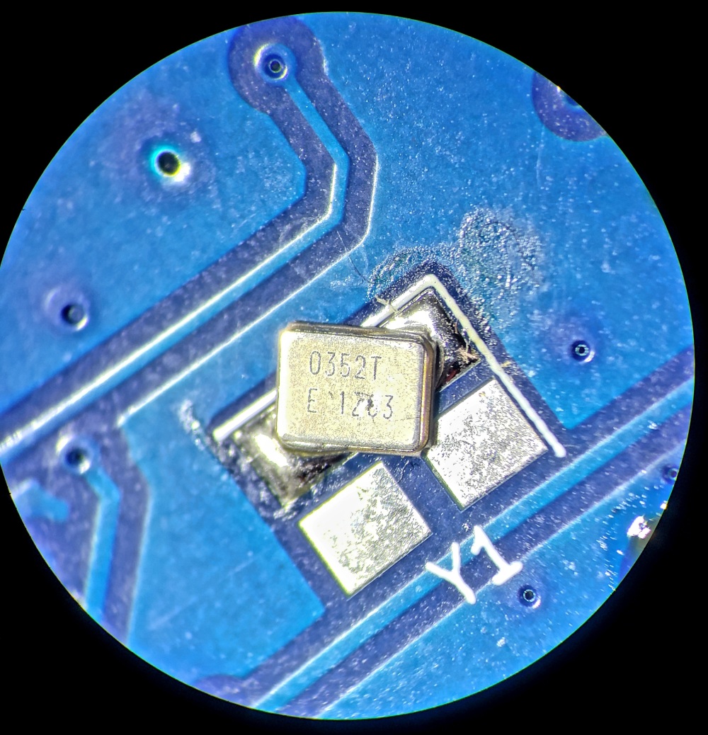
Once again (ugh) I confused the footprint situation on the crystal for the Si5351’s reference, and had to make some lemonade. At least crystals don’t seem to mind being crooked that much :-).
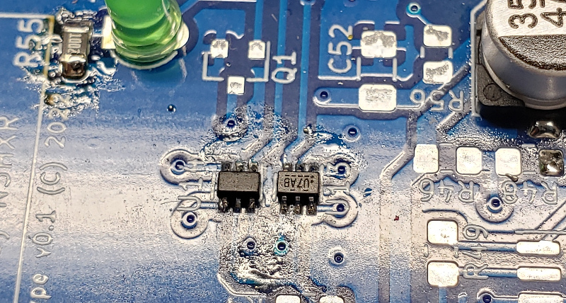
The second gaffe came with the Si5351 outputs. The chip has three oscillators, and I need six for the board – two IF mixers, an IQ mixer to baseband (needs two), and the IQ modulator for TX (another two). So I’d worked out a switching architecture, where the first two outputs are shared between the IF mixers and the TX IQ modulator, and the third output goes to a 4x divider to generate quadrature signals for the final AF baseband mixer.
But I made a copy-paste error on one of the little FSA3157 switches for routing the oscillators, and it was exactly backwards on the board. Fortunately (thank goodness) the footprint is kind of symmetrical on the FSA3157. If you look very closely, you can see that one of these switches is flipped upside down and “dead-bugged” onto the board :-):
There was one other pretty significant mistake on the TX side – I had a complete lapse and didn’t realize in schematic capture that the DACs are SPI, not I2C, so I had to run some bodge wires on the board to connect them to the right pins on the microcontroller.
But after that, things went quite well in general with very few modifications.
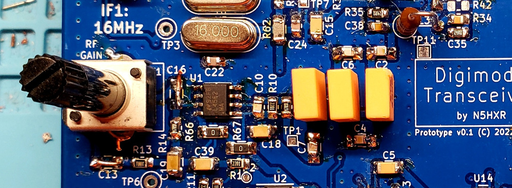
Tour: First IF
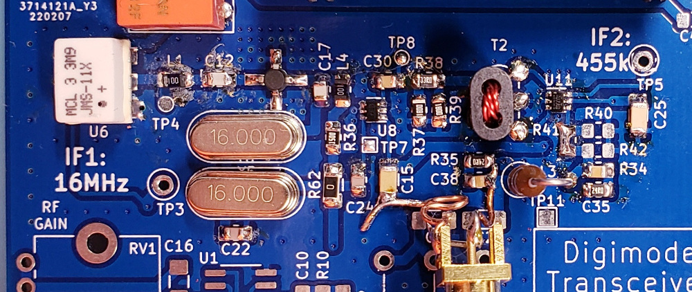
The first IF starts with a JMS-11X mixer from Mini Circuits. I used it mostly because Mini Circuits ran out of stock on the ADE-1+, which I’d used previously. This one is a very nice mixer, though the J-leads are somewhat more annoying to solder. I didn’t really expect that, actually, so I ended up working out its installation with hot air instead of an iron.
From there, we go right to a MAR-6SM+ MMIC amplifier, with about 20dB of gain, and then into two 16MHz crystals as a “roofing filter” of sorts. After this filtering, I added one of the little BGA2866 amplifier blocks I’ve used before.
I ended up running into some oscillation issues with the BGA2866 in this case. But, different from the last project where I used it, I now have a spectrum analyzer. It was easy enough to probe the board with the analyzer, and see spikes way up in UHF ranges. I believe in this case I saw oscillation around 520MHz. I ended up swapping out the 0-ohm resistor at R62 (visible in the photo, which was taken before the swap) with a 1206 ferrite bead. Easy fix!
Tour: Second IF
The second IF starts with an FSA3157-based switching mixer. This was an experiment – I’d reasoned through it based on reading up on mixers, and done some testing in LTSpice. I’d used them in my IQ modulator experiment, so I was confident it should work as a mixer here.
It certainly works, though I suspect I’m getting more loss at the mixer than I expected. LTSpice simulations suggested something like 6dB of loss, but I think it’s more like 8-10dB on the board. I don’t really know why – perhaps one of these days I’ll take one of the spare boards from JLC to build just this piece and do some more thorough testing.
From the mixer, we have signals at 455kHz coming in, through a diplexer to terminate high-frequency products and pass the low ones, into a ceramic filter. This ceramic filter uses cheap ceramic resonators, and is directly inspired by an article in QEX I’d read. I have about a hundred of these 455kHz resonators around, and they seem to work just fine.
This gives me a selectivity of about 2kHz, which I thought would be decent for digial modes. It turns out to be quite passable for SSB reception, as with only three resonators it’s not incredibly sharp.
We now pass into an LM4562 opamp for additional gain. This is a fairly normal inverting amplifier configuration, but with a logarithmic potentiometer for variable control in the feedback path. My selection of components gives me a range from about -10dB to +30dB of gain. Playing with it, having that 40dB of range is pretty cool.
Tour: Baseband Conversion
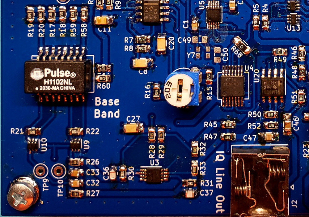
Finally, we come to a 6dB attenuating splitter that feeds into one of my Ethernet transformers. These are very inexpensive, and have usable bandwidth from about 50kHz well into VHF (nearly 200MHz, in my testing). So, for about $0.20, I didn’t have to wrap any toroids or worry about balance issues here – a nice win, I think!
Each of the transformers comes out into another FSA3157 switching mixer, driven by the quadrature division of the Si5351’s third oscillator output. These worked great, and feed directly into a couple opamp stages that give me some control of the AF output at the phono jack, and into the ADC pins on the Teensy 4.0.
Tour: TX Chain
![]()
The transmitter side is a software defined radio, with the microcontroller driving two MCP4802 DACs: one for the in phase channel, one for quadrature. In retrospect, I think I should have added an opamp gain stage to raise the voltage closer to the rails, and buffer a bit better into the mixers. But it turns out to work just fine as it is.
After the DACs, I and Q signals enter two FSA3157 switching mixers driven by the Si5351’s first and second oscillator outputs. These dump into an RF combiner, which feeds a push-pull stage for power amplification using two 2SK3475 transistors.
Here, I encountered some UHF oscillation as well, and once again used the spectrum analyzer to diagnose and find spikes on the collector pins for the power FETs. After consulting with some of my mentors, I scraped up some solder mask and soldered a 100pF capacitor in shunt at each collector. This eliminated the oscillation entirely, and resulted in a functioning power amplifier.
My suspicion is that by feeding the collectors with big inductors for HF use just puts their inherent capacitance in a really good place for self-oscillation. They are, after all, designed for UHF operation. I think I want to experiment with using them for a VHF project, where I’ll use smaller inductors on the collectors, and probably won’t run into these issues.
From the PA, we go out through a QRP Labs low pass filter module, and off to the antenna!
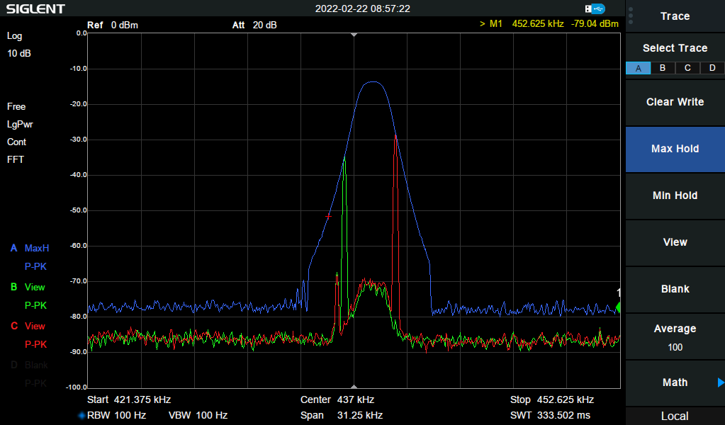
Alignment and Testing
Once I had everything put together, I had to align the IF stages, and validate that it could transmit legally. Here, the spectrum analyzer came in handy, as I worked out the math and moved things around with the LO frequencies to center the pass band on both of the mechanical filters:
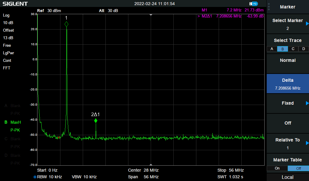
And on the TX side, I checked harmonics with a tone on the 40m band. Things came out very nice, with the harmonic at 14.4MHz down at -64dBc! I’m quite happy with how this came out.
And with the DAC-driven IQ modulator, I should be able to shape very nice pulses and keep my key clicks and sidebands down. I worked up a little CW transmitter firmware, and checked the waveform shape:
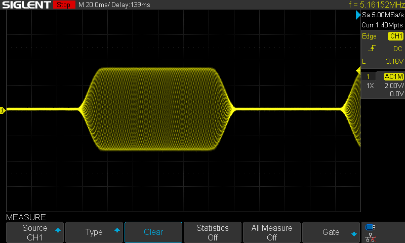
Can’t beat that, it came out quite beautifully!
Receiver testing
Before trying to transmit, I thought I’d run the receiver overnight with FT8 (an easy source of signals for testing!). Here’s a map of received signals from GridTracker, with the overnight pass on 40m:

The receiver isn’t quite as sensitive as I’d like – I experimented with an RF preamp in front of the board of about +17dB, and thought that was a lot better. In a future revision, I’ll probably tweak the gain distribution. I think it was around this point that I started questioning the insertion loss of the FSA3157 mixers. Some future experiments might illuminate why my gain calculations came out somewhat short.
Transmitter Testing
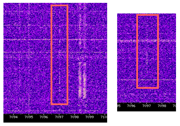
Using the CW sketch I’d written, I thought I’d try some transmitting. The PA only gets me about 230mW of output, so it’s definitely low power! I didn’t have much confidence that I’d show up on RBN or get picked up by an actual listener. But as the photo above shows, I did show up 1,700 miles away on a WebSDR in Utah, which was very encouraging!
I adapted my old code for Hellschreiber transmit, and rigged it up as a little Hellschreiber beacon – just sending my a short message about testing a homebrew hellschreiber and my call sign. I was able to use the Corrinne, UT WebSDR to receive my transmission and demodulate it in FLDIGI!
![]()
Wow, couldn’t believe how well it came out! I couldn’t wait to start playing in the software domain, making DSP modulators and demodulators to make it a useful digimode transceiver.
Conclusions
This post shows the hardware build, which was plenty of effort as it is. I’ll be following this up with some posts about the software side – as a full RX and TX SDR transceiver, this should be a good platform for learning some DSP stuff that I don’t know yet :-).
I am generally happy with how things went, but I think I’ll continue to a revision of this design with some changes based on my testing:
- I think I’ll ditch the MMICs. They give the impression of ease of use, but they’re somewhat overkill. I’m now actually thinking I can replace them with high GBWP opamps and have lots of control over impedance matching and gain.
- I may or may not continue with the double conversion architecture – it’s not really necessary, and a single conversion IF would be a simpler and smaller board. I like some of the advantages of this design, but it’s somewhat overcomplicated.
- I need to revisit the mixers, as I think they’re lossier than LTSpice suggested. Some experimentation is in order.
- As I said above, I’d like to add a layer of amplification / buffering in front of the DACs. I should be able to get over half a watt out of the 2SK3475s, and I think part of the issue is I’m just not able to push them hard enough.
Anyway, this was a monumental undertaking at this stage in my RF engineering journey, but it is a massive success, and can’t wait to see what I can learn by playing with it. Building things that work is fun!