Building a Backpack for an ADF4351 Board
I’m playing around with some ideas for VHF and UHF experiments, and need a good signal source. Before implementing a fancy PLL myself on my own boards, I thought I’d pick up an ADF4351 board from Amazon. I could poke at it with my Bus Pirate, but that’s not really a viable approach for making benchtop experiments easy in the future!
So I designed a “backpack” control board to mate with the ADF4351 board that embeds a microcontroller and a USB serial interface so I can make a much friendlier user interface. This post walks through the process and results.
Introduction
It’s easy enough to make an oscillator for HF from component parts. And there are a lot of synthesizer options that are quite popular for homebrew projects – e.g., the Si5351, which I’ve used quite a bit, or the AD98xx series. These are reasonably inexpensive and easy to work with.
But what do we need if we want to try VHF and UHF bands? Even the 2m band is beyond the Si5351’s practically usable range, as its phase noise and other flaws really affect its viability. And then what about 70cm and beyond? For these bands, we need a more sophisticated oscillator, and the main solution is a phase locked loop (PLL). The Si5351 is such a thing, just not designed for higher frequency RF use.
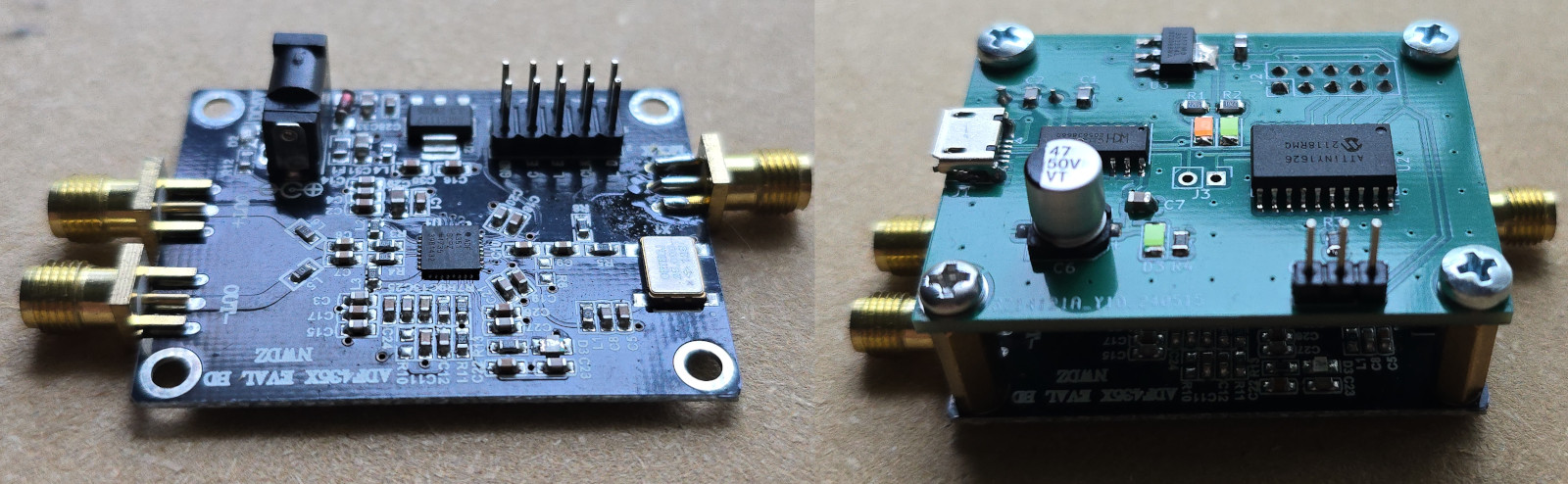
Various manufacturers make RF-capable PLLs, but Analog Devices is more or less the source for standard selections. The better NanoVNAs, for example, use the ADF4351 PLL as their signal sources to get up into UHF. These chips are not exactly cheap, but you pay what you get for, I guess :-). I found a nice ADF4351 experiment board on Amazon:
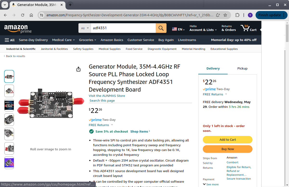
These are basically a clone of the very expensive Analog Devices ADF4351 Evaluation Board, which runs over $200! This was actually the second board I tried. The first one was one you will also see from the popular sources (one of these), but it was defective, and wouldn’t reliably lock. I tried a few things to fix it, but was unsuccessful, and switched to the board depicted above, which has worked nicely.
Configuring the PLL
The PLL has tons of features, and is much more complex than getting the Si5351 working. The PLL configuration involves calculating and writing the values of 6 32-bit registers over its SPI bus. This bus is write-only, and selecting the values is very complicated, with multiple solutions for a given frequency that have various pros and cons.
Analog Devices does provide a fancy software tool for their evaluation board, downloadable here. As you can see in the screenshot below, you can adjust all the various features of the chip and generate the register values:
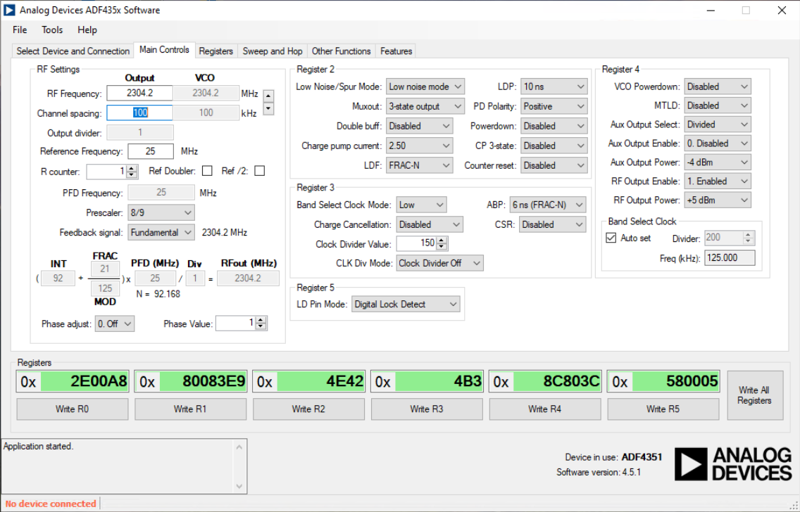
This works fine if you have a well-defined use case, and just need to configure some target frequency, maybe with a set number of channels with even spacing. But it’s not the best for an experimenter. If you want to choose arbitrary, fine-grained frequencies, such as to behave like a VFO, it’s really annoying!
Unfortunately, calculating correct and optimal values for these registers given a target frequency is not for the faint of heart. There are some projects on github that do it, and they do work. But they tend to make some starting assumptions or ignore consequences of some configuration details. So for the time being, I’ve put off learning how to do that in a good way until I have some more experience with the chip.
My first tests used my Bus Pirate to interface with the SPI port on the ADF4351 to write register values generated from the Analog Devices software depicted above. But this was a rats’ nest of wires and bound to the Bus Pirate’s interface. I figured I could wire up a microcontroller board, but then I’d have wiring, maybe a breadboard in the mix, and thus would not be an ideal module to use for benchtop experiments.
I decided I wanted to build a backpack for the ADF4351 board that would give me convenient interface to configure the chip.
Backpack Board
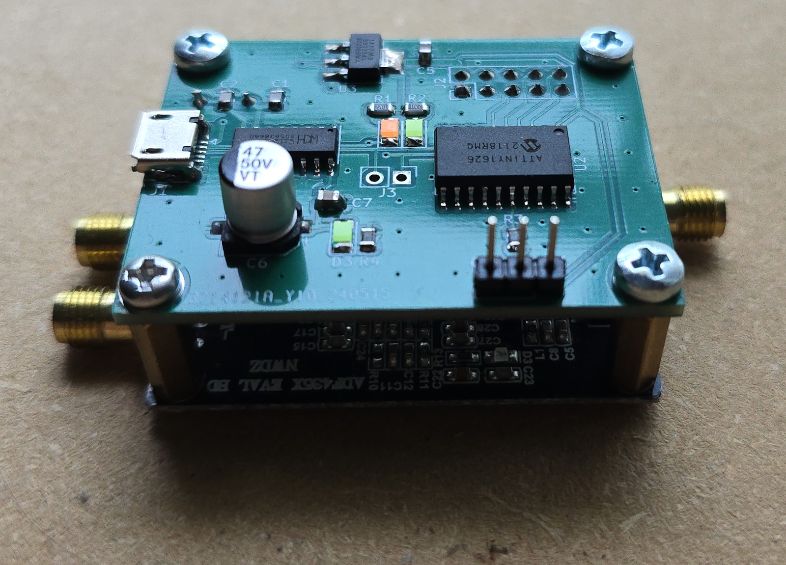
I’ve built a lot of microcontroller + USB interface projects now, so it was pretty easy to just copy and paste elements from other projects to make this one. The main thing was to build everything around a “mezanine” connector, which would just be a 2x5 female pin header that has to be in just the right spot to connect to the ADF4351’s corresponding male pin header for interfacing the pins:
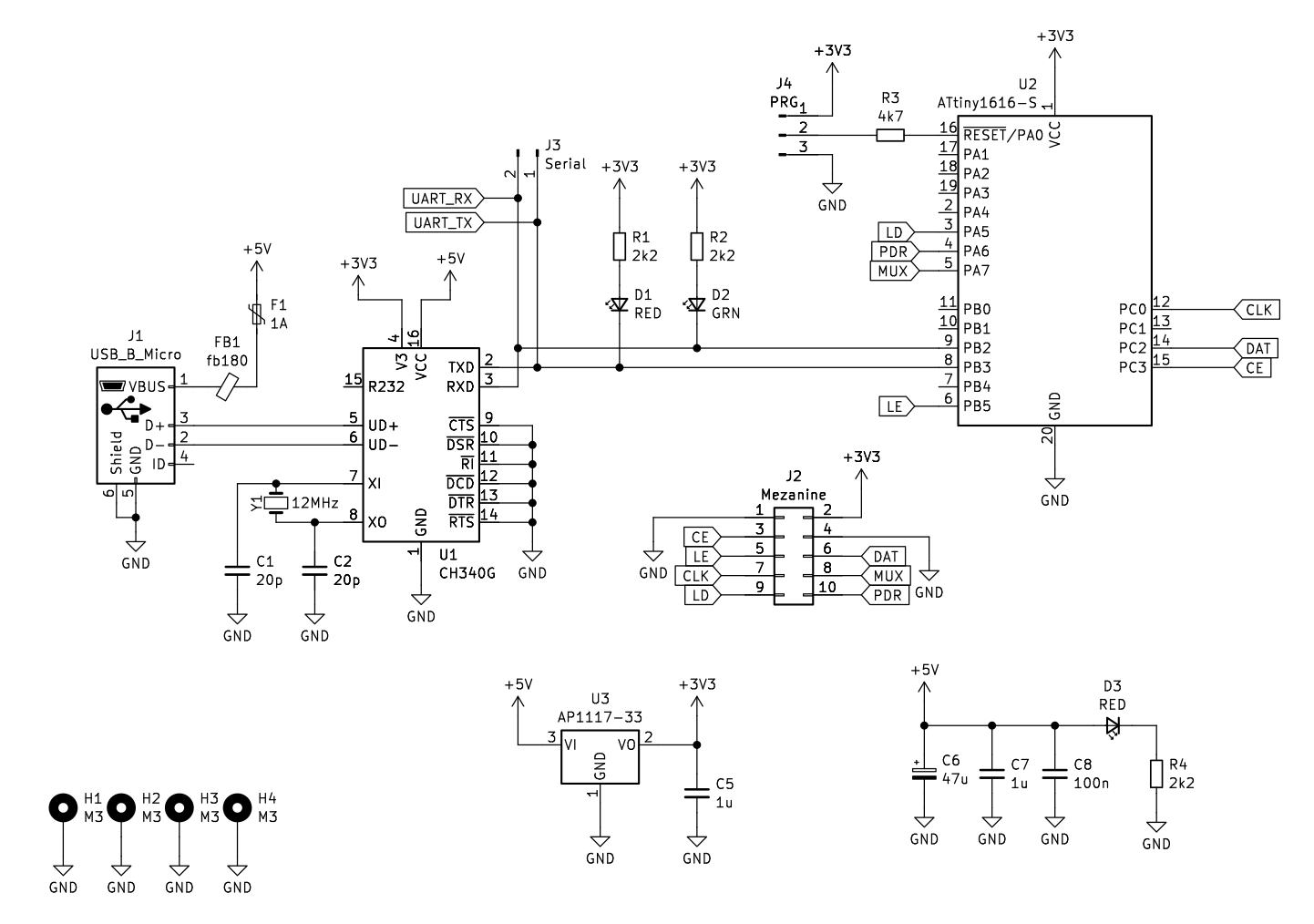
The summary is that we have an ATTiny1626 microcontroller to configure the ADF4351 and a CH340G USB serial interface. Power is supplied through the USB into a 3.3V linear regulator (but can also be supplied on the programming header). A few LEDs to make it pretty, and that’s about it!
Layout of the board involved taking careful measurements of the mounting hole locations and distances to the 10-pin header. I ordered the board from JLCPCB along with a bunch of other projects I had going, and it finally arrived.
Assembly went quite well, with no issues. Since I started cleaning my boards in the ultrasonic cleaner, I am very happy with the results – no flux residue at all, and everything looks pristine. The only real problem came up when I discovered that my UPDI programmer for the ATTiny1626 was misbehaving, and so I had to write the jtag2updi programming firmware to a new Arduino Nano, and everything was working great.
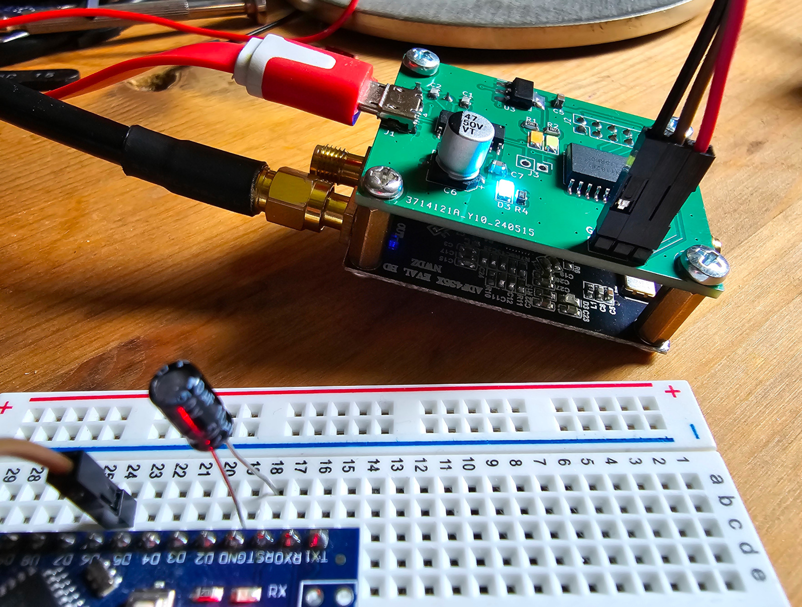
The board attaches as shown below:
Firmware
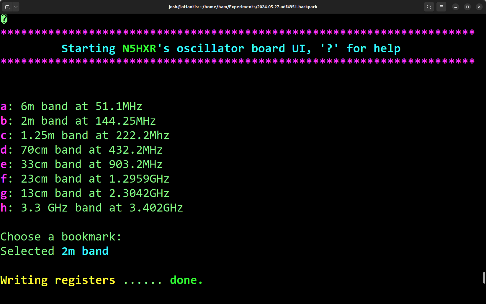
Since I’m waiting to work out an optimal strategy for calculating register values for a VFO-style configuration paradigm for the ADF4351, I wrote an Arduino sketch (source code here) that just lets me load register values. It also has some “bookmarks” built in to easily select an output in all of the VHF/UHF bands that are supported by the ADF4351 (it’s quite a few!):
In the future, I’ll probably add storage of the configuration in EEPROM so that the board only has to be powered to function. I also put in some breakout pins for the UART, in case I want to control this board from another microcontroller in a larger project, and skip the USB part.
Testing
I terminated the ADF4351 board’s output into my spectrum analyzer, and played with setting different values for the registers. I worked out an initial bookmark for each relevant ham band. Here are the views on the scope for 6m, 2m, 1.25m, 70cm, 33cm, and 23cm. I also generated values for 13cm and the 3.3GHz band, but I can’t see those on my analyzer :-(.
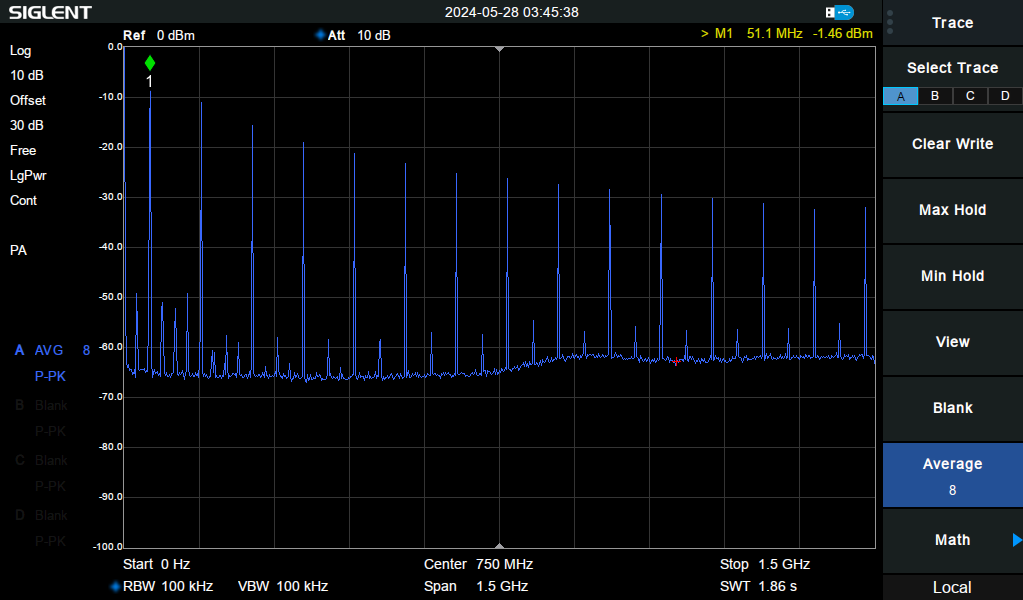
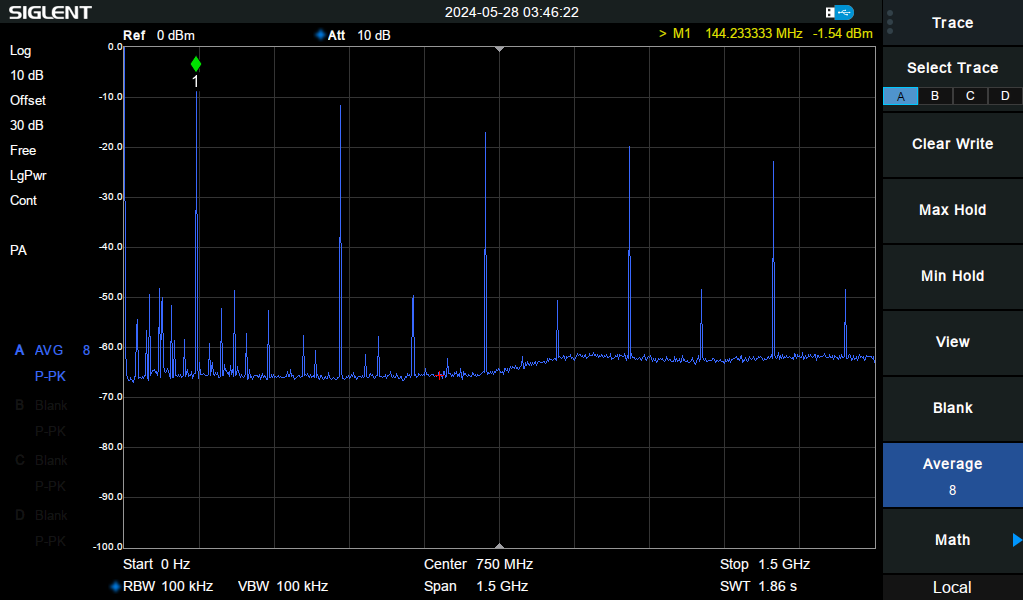
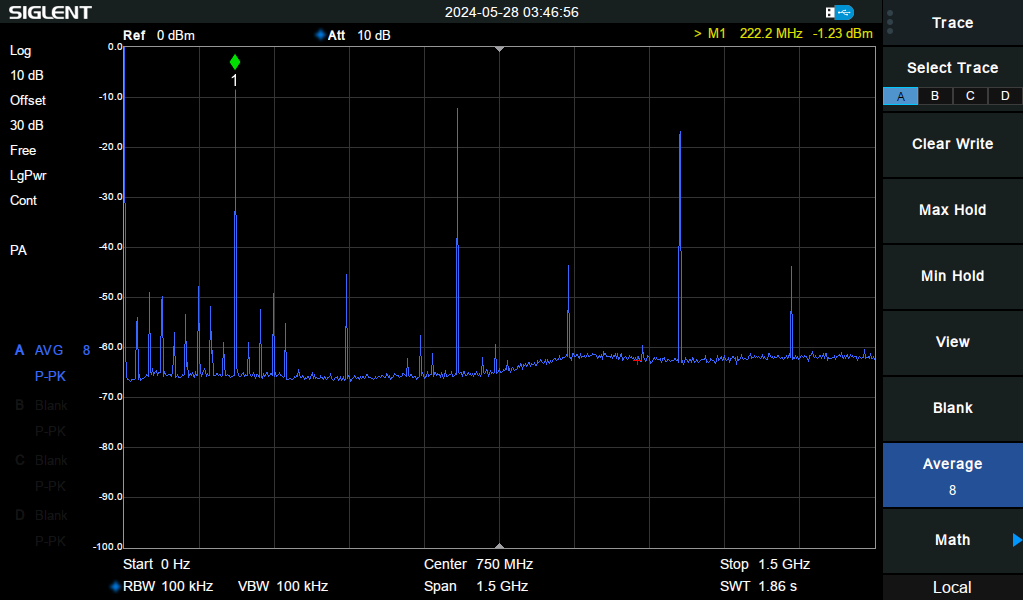
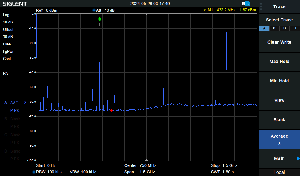
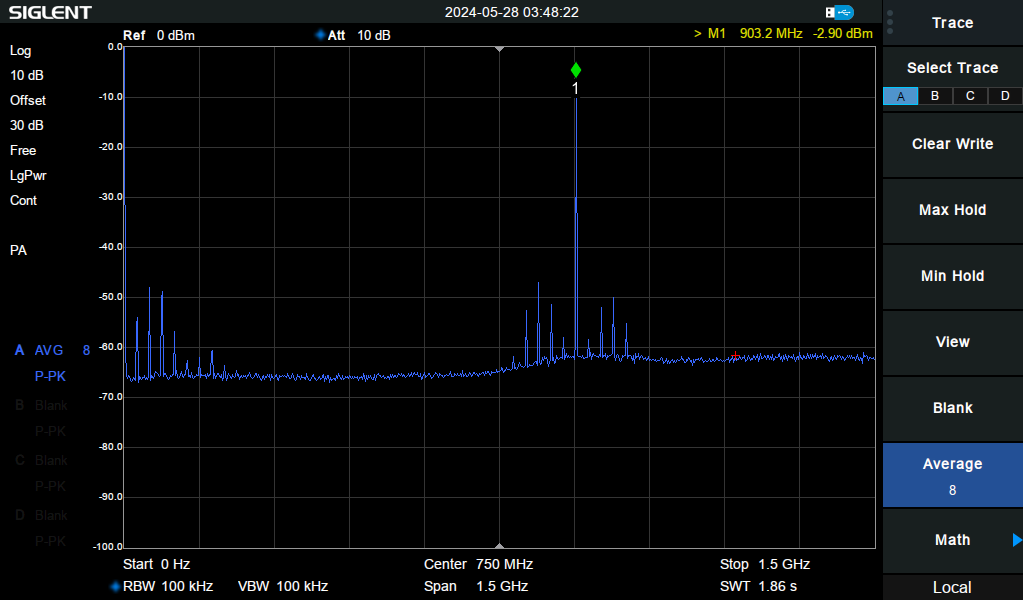
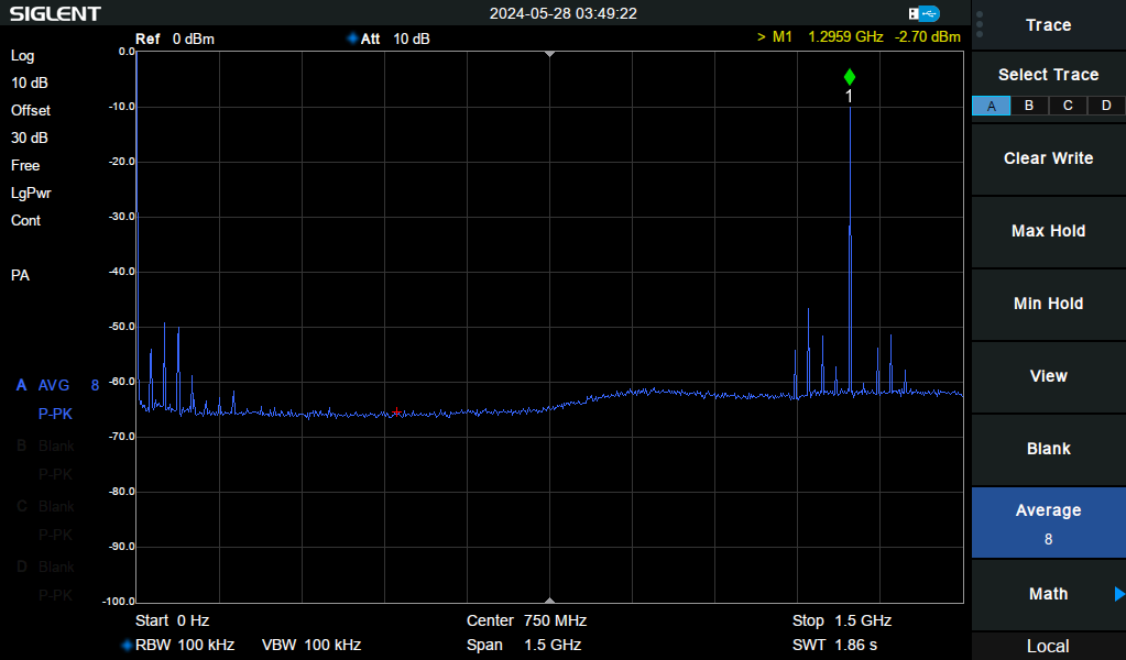
I have set the chip for maximum output power, but I’m only using one side of the balanced outputs. Furthermore, I believe the output network on this board is minimal, so there’s no matching for optimal output. So I end up seeing about -2dBm. This is OK, because even at the stated output of 4dBm, I’ll still need to buffer and amplify the output from the chip to drive some of the mixers I plan to use (mainly diode ring mixers from Mini Circuits).
I’ll also have to work out some filters. Along with this board, I also ordered a board made that should be a 2m bandpass filter, but it did not work out well. I have some things I need to learn about VHF/UHF filters!
I do see some defects in the output. I believe that there are several possibilities – poorly optimized values for the PLL configuration, a low quality onboard reference clock on the ADF4351 board, etc. I picked up a really nice OCXO 10MHz reference that I will experiment with, and see what impact that has on signal cleanliness.
Anyway, this is a great foundation for starting to explore higher bands. I’m looking forward to improving the firmware on this board so that it does the hard part of calculating values for VFO-like behavior, which will also teach me a lot about the performance metrics for PLLs.