DIY Load Pull Analysis
This blog post is about the first step in what feels like a big project for me – but one that I hope will resolve a lot of outstanding questions I have about impedance matching and power amplifiers. This is my journey to create an in-home DIY load-pull analysis lab for characterizing and understanding transistors.
Since I started on this ham radio home brew journey, I’ve been unsettled by many questions about impedance matching. A lot of this comes from early frustration trying to build RF power amplifiers with the wrong transistors. To make it more confusing, I started reading about differences between small signal behavior and large signal behavior, and clues that normal rules don’t apply in nonlinear operation.
After I tried to get some answers, someone told me it’s not uncommon to just guess one’s way around to arrive at the desired performance. And yet, I could easily find material from college courses, conference presentations, and other professional RF engineering sources that suggest that there are ways to measure and design these things without the assumptions and guesswork. But the equipment is prohibitively expensive, and manufacturers don’t usually give you the data you need for HF amateur radio homebrew use.
I eventually stumbled onto a few key resources – RF Power Amplifiers for Wireless Communications by Steve Cripps, as well as NXP’s AN1526 – which discuss the load-pull analysis technique, and some other methods for characterizing transistors. Load pull is very common in professional RF engineering, but almost exclusively the domain of high frequency UHF and microwave situations. I wondered if the same approach could work at HF, and help me explore some of my questions.
I found those resources very illuminating. Here are the highlights:
- Small signal measurements do not predict large signal behavior
- Large signal behavior varies by frequency, operating point, and drive level
- Anything that’s not class A operates in the nonlinear region, affecting results
- Maximum power or efficiency is not necessarily correlated with minimum VSWR
Since almost all of the texts I’ve ever read on designing amplifiers are built on small signal models, it’s fascinating to find explanations for a lot of the things that didn’t make sense to me about RF power amplifiers. The NXP application note sums it up this way:
This is the basis for much of the black magic that surrounds RF power amplifier design, but the reality is the circuit designer is plagued with a paucity of good design data, and a lack of adequate tools to make the initial design “foolproof”.
Load Pull Analysis
The application note has a straightforward definition of what load pull analysis is: “A variety of load impedances are presented to the device … the performance of the device is measured at each one of these points.” A lot of load pull setups are really expensive because they can be largely automated, and involve a bunch of expensive equipment (especially for very high frequency work).
So, you try a bunch of input and output impedance matching solutions, recording how your device performs. The measurement can be whatever you are chasing – power output, IMD performance, efficiency, whatever. The point is that you kind of handwave over all of the complexities that make large signal behavior weird, and empirically map out how the transistor behaves. You have to do this at the operating point and drive level you intend to use, as many of the confusing large signal behaviors vary because of those factors.
In the end, you can map out your device’s behavior, test multiple devices, average results, and develop a picture of what sort of matching networks will work best for your situation. It’s not pure theoretical science, but it’s an empirical approach that at least provides a systematic method that can generate results.
The DIY Setup
I’ve recently (finally) acquired all the parts to put this thing together. I’m not going to lie – it’s not cheap. But there’s a big difference between this setup and a commercial load pull arrangement. I’m talking thousands (maybe tens of thousands) of dollars difference!
I already had a bunch of the components I needed. I already had a decent oscilloscope and signal generator, as do many hobbyists. But I had to add a few things to the home lab to get it all together. Here’s the basic architecture:
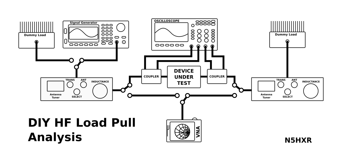
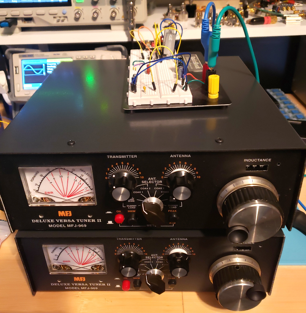
At first, I was going to get some cheap antenna tuners with tapped inductors. As I thought through the problem, I figured I’d want more granularity than a tapped inductor would provide. After committing to two roller inductor tuners, I’m very glad I didn’t go with tapped ones. In fact, I was going to make my own tuners. But when I investigated the cost of roller inductors… wow… it doesn’t cost much more than a roller inductor to just buy a whole roller inductor tuner. So yes, the tuners are $500 (two MFJ-969s), but that’s the bulk of the expense getting this up and running.
For practical considerations, I’m not really convinced that the directional couplers are necessary. It does make it possible to observe the forward and reflected waveforms, and maybe tune more precisely for VSWR. But I initially just set things up without the couplers, and monitored output power at the dummy load on the oscilloscope, and didn’t at any time feel the need to use the couplers. Maybe I’ll change my mind about that as I learn more though.
The First Test
Having unboxed my tuners, and wired everything up, I couldn’t wait to try something. I have my IRF614 amplifier I’ve been playing with handy, so I put it immediately to use. It’s not the most ideal test fixture, being on a breadboard with flying leads, etc. But I just wanted a quick proof of concept to see if this crazy idea was going to work at all.
First, I tested power output with the bias set where it was from the last time I used it. I figured I wouldn’t put too much effort into tweaking stuff, as it’s a DUT after all. It’s supposed to be a “black box”. Before tuning anything, I saw that its unmatched output was 5.03 Vrms into a 50 ohm dummy load. That’s 506mW – and this was at 1 Vrms input from my signal generator, which I’ve previously verified does have a good 50 ohm output impedance.
I twiddled the knobs on the tuners. Each is a variable T-network, with two series capacitors and the big roller inductor in shunt configuration. It was really interesting playing around – I could clearly see that there is a relationship between both input and output impedance matches. I guess it’s a termination sensitive amplifier (TSA?).
After some playing around, I was very glad I had the continuously variable inductors. I could make small adjustments to each knob in turn, seeking increased output on the scope as I went. I finally dialed it in to 7.12 Vrms. That alone was a pretty neat finding, and I know that if I’d only tried tossing some inductors or capacitors in series or parallel at the output, I would never have realized so much gain because there is a cooperation between input and output. The setup was really starting to make sense!
So at 7.12 Vrms, that means I’d managed to take the amplifier to a full watt of output (!); a full 3dB improvement, just by matching the input and output. But… I wondered… can I now swap in the VNA and measure a dummy load where the generator was, and the output network, and quantify what the setup was?
I did so, and found that the sweet spot was at 15.1 + j11.6. On the VNA, I could see where it was on the Smith chart, and I spent some time moving the load around, then swapping back to the amplifier, and confirming that everything was repeatable and predictable.
Building a -3dB Contour
So, one of the things that I’ve read in the literature is that you want to get a contour map of your device. Once you know the peak for your target performance parameter, there will be an infinite number of matches that are “worse”. For example, if you’re seeking maximum power output, then you can define some less satisfactory level (like -3dB from the max), and map out a bunch of different matching networks that yield that value. Those can get plotted on the smith chart, and you get a visual representation of your device. That sounded simple enough :-).
It was a real adventure trying to figure out how to move the load in specific directions. I think this might be a consequence of the variable T-network, but some regions of the smith chart are a lot easier to hit than others. I’ll be experimenting with how to become more efficient at mapping out the smith chart in the future, for sure!
But, with some effort, I worked out a few strategies for moving off of the maximum load and arriving at a -3dB point. In this case, I was basically looking to create a bunch of data points in different directions that would yield 5 Vrms into the dummy load. After laboring intensively to figure out how to plot points on a smith chart (ugh, there’s definitely some work to be done on open source smith chart plotters!), I ended up with the following:
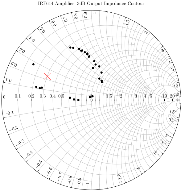
Wow! It’s not perfect – I had some variability due to my setup (I don’t have the ideal set of connectors and cables, for one thing, and of course the amplifier has no thermal stability, and it’s on a breadboard!). But I can definitely see the oblong / elliptical shape of the -3dB contour. It bears enough resemblence to real examples of load pull contour maps that I’ve seen, that this result gives me some real confidence that this is a valid avenue of inquiry!
Putting it to practical use
So… knowing how my amplifier performance maps out is cool and all. But could I actually make use of this information and improve my amplifier? It would be nice if I could bump up the power without the big roller inductor tuners. So… I visited one of my favorite matching network design sites and plugged in my solution. I chose an option that I thought I could whip up quickly, and set to work.
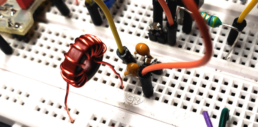
My results were interesting. I got kind of close to where I wanted – certainly improvement. I hit about 6.4 Vrms, about 820mW. Not quite the 7+ Vrms that I could get with the tuners. I measured the network against a load with the VNA, and it was pretty close to the spot on the smith chart where I found the ideal spot. But the exact peak is pretty narrow – with the continuously variable T-network, it took some delicate manipulation to squeeze out the last couple dozen millivolts…
There are probably some other reasons that I couldn’t quite bump it to the perfect sweet spot. I only have so many values of capacitors around, and tweaking the inductor only gets so far. I checked the Q of my inductor and capacitor together on my spectrum analyzer, and saw that the difference between these cheap caps (of which I have many values) and a nice C0G SMT cap (of which I have very few values…) is huge (20 vs 120, in today’s case). So I suppose if I ordered some nicer parts I could squeeze a bit more out.
Conclusions
I’ll consider this a great success! It’s my first time ever even trying this sort of thing, with a bunch of test equipment that’s new to me, and I managed to get some nice initial results. Before this, I wasn’t even really sure if this kind of experimentation was useful.
The next step is to put some real effort into making good test fixtures. My breadboard amplifier is a decent black box, but it’s not a good way to really quantify a transistor. I need to rig up a fixture with minimal parasitics (no breadboard), and a better design to isolate the transistor (better bias network), and some thermal management (if not thermal compensation, at least a big heat sink!). I think this will dramatically improve the precision of my results, as well as make for results more useful in designing an amplifier outside of the fixture.
It was very educational seeing the changes when adjusting the matching networks. I don’t know if the variable T-network is ideal… it’s just what’s easily obtainable at the moment. I imagine some other architectures might be better for getting out to the corners of the smith chart. For nicer transistors than the IRF614 I know that the sweet spots are likely to be close to the rim! I may ultimately end up building my own tuning stages too; we’ll see.
And finally, this was lots of fun. I feel like doing this is going to help demystify some aspects of RF power amplifiers that aren’t written about much at the hobbyist level. I’m really looking forward to the next experiment with this equipment.