Tweaks for push pull gate driver amplifier
Continuing from my successful attack on thermal issues, I did some more measurements of the amplifier. I’ve now tweaked a few things that improved some more issues. The result is a little more power, a little better efficiency, and some improved (and safer) operation.

Parasitic oscillations
The first thing I noticed when I started more organized measurement of the amplifier is that the IRF510 drain waveforms exhibited some wild oscillations. I am kicking myself because I didn’t take a picture of the waveforms before I worked out a fix, but imagine you have a decent 7MHz square wave, but with a 20 Vpp 52MHz sine wave superimposed on it. Yuck.
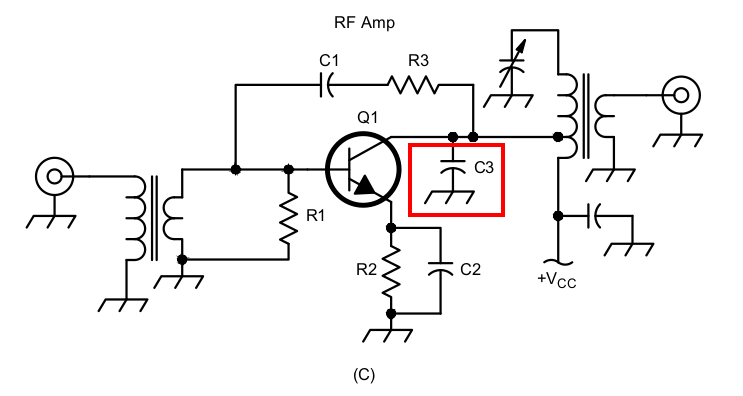
Looking through the ARRL handbook, chapter 17, which discusses handling parasitic oscillations, I worked out what my options might be. I didn’t think I could fit a ferrite bead on the drain, and I didn’t want to try to add some negative feedback. One of the handbook’s suggestions looked quite feasible – bodging in a capacitor on the drain:

Since I just learned some things about capacitors, I thought I should put one of my new TDK 450v NP0 capacitors in there. I only have two values to choose from (690pF and 1nF). Figuring the oscillations measured 52MHz on the oscilloscope, the 1nF value seemed like it might be a good choice, at 22R at 7MHz and 3R at 52MHz. Through the transformer, I guess my load is about 5-6 ohms, and the output impedance should be quite low on the IRF510s, so I thought this matched the handbook’s suggestions as well as I could.
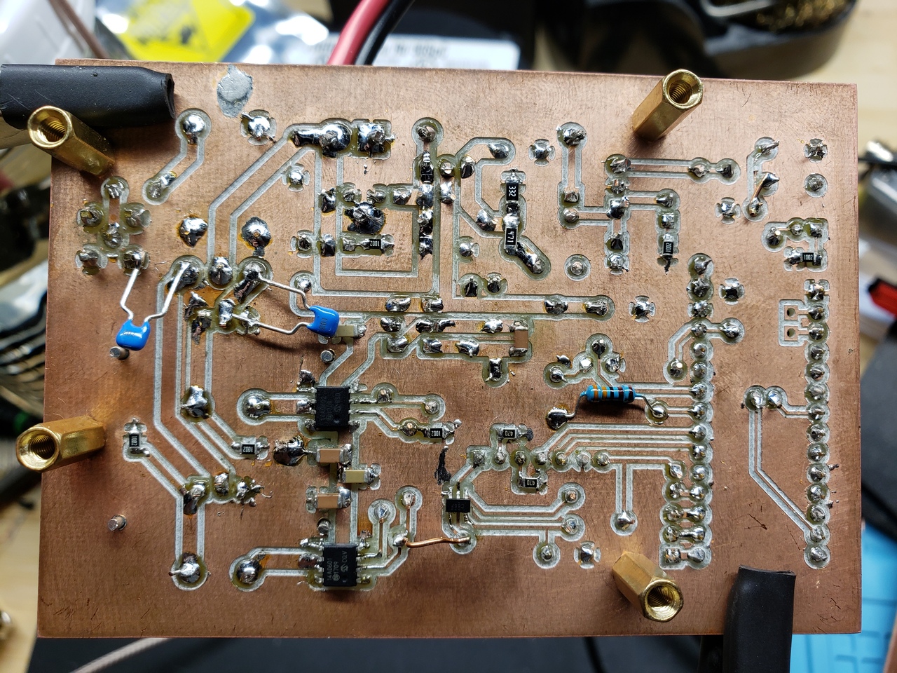
Once I added the capacitors, the oscillations were basically gone (OK, there’s a little wiggle in one of them, but not nearly what it was!). What was more interesting was a concomitant increase in power, and a drop in total current consumption by the amplifier:

This yielded a decent 19 watts of output at about 56% efficiency – up 3 watts and 10 points!
Pull downs on the gate drivers
Another thing I noticed with repeated testing was that every time I would power the board, there would be a burst of current draw. I reasoned this was because the MCP14A0601 has internal pullups for its ENABLE pins:

This means on power up they are turned on, and with the default startup state of the Teensy LC’s output pins, it happens that “no signal” is very briefly passed to the inverting gate driver, which slams its transistor on. It didn’t cause any damage because this pulse was very brief (just long enough for the microcontroller program to set the pin states to their proper defaults).
But it was annoying and unsightly, so I added a pull-down resistor to the ENABLE signal into the gate drivers. According to the datasheet, the integrated pullups are “typically” 1.8 megohms. I went with 6.8 kilohm resistors for my bodge pulldowns, so my resistors would win in that little tug of war. This cured the board of this startup behavior, and I feel a lot happier with this configuration.
Squaring up the gate driver input
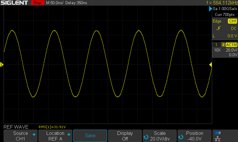
A much earlier test board with the MCP14A0601 had made me a little leary of passing the local oscillator directly into the gate drivers. I had observed some instability, and I wasn’t sure if there was some oscillation at these frequencies. So I’d tentatively put a 47 ohm resistor inline between the two. Well, after scoping the traces, I saw that this was making the signal a very slewed sawtooth wave. So I bypassed this resistor (R6 on the schematic), and it square up nicely.
Duty cycle issue remains
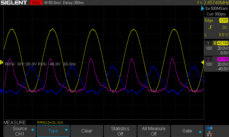
In testing with my previous iteration of the amplifier (a single IRF510 and gate driver), I had found that the gate drivers increase their duty cycle as the frequency goes up. In that testing, I’d found that these work OK at 7MHz, but at higher frequencies (e.g., 14MHz), they became fairly unusable. The duty cycle issue is still there, and can be seen in the following image from the oscilloscope:

Notice how each drain (the magenta and blue waveforms) spends more time at low voltage than at high voltage… this is directly because of a similar duty cycle issue from the gate drivers.
For now, I’m getting 55% efficiency or better, and getting an unbelievable 18 watts out of this amplifier at 12v supply. If I go forward with this design to make a 40m transceiver, it will be perfectly fine. It will exceed my own expectations for my first “full suite transceiver” project.
But, in the future I may want to follow through with one of my ideas earlier – experiment with different gate drivers and see if there is one that might do better at higher HF frequencies. I’ve even noticed some of them have both an inverting and non-inverting output in a single chip, which could reduce parts count by one whole chip (more than making up for the slight increase in price for those fancier chips).
We’ll see… I kind of like these gate drivers, and if nothing else I’m making amplifiers that don’t look like other ones I see, so I’ll keep playing with the idea.
Conclusions
With this testing, I think my search for a power amplifier chain for my mid-term portable digital mode transceiver project is at an end. I’m happy to proceed with a 40m solution, and the output level is more than adequate. I also suspect some things will clean up a bit when I make a 4-layer PCB with a proper ground plane. Since I’ve observed and fixed a few parasitic oscillation issues, I know what allowances to make in a final build, so I think this is buttoned up quite nicely.
Up next is to start learning receiver stuff. I’d previously played with a Tayloe detector, but I’ve been reading up on more traditional single conversion superheterodyne designs lately. I might put together a couple side-by-side receiver builds and see which direction seems best for my first transceiver project.